Comparison of DCR Current Sense Topologies
Abstract
Current sensing plays an important role in DC/DC regulator systems, especially in multi-phase buck converters for CPU VCORE applications. In VCORE applications, the current signals are used to decide the load-line droop, per-phase current balance, current reporting, and over current protection. Moreover, if the control topology is current mode, the current signal will directly affect the system stability. Therefore achieving accurate current signals is very important.
Generally, the inductor DC resistance (DCR) current sensing technique is widely used in CPU voltage regulator (VR) applications due to its lossless characteristic. However, the DCR current sensing method needs to parallel an RC network beside the inductor, and is likely to be near noisy nodes like the phase node or other PWM signals. It offers many opportunities to add noise which may decrease the current sensing accuracy. In addition, the offset and bandwidth of the current sensing op amp can also decrease the sensed current signal accuracy or distort the current signal, and generally present a great challenge to acquiring a clean current signal.
In this application note, two kinds of current sense methods for multi-phase regulators will be introduced. One is the differential current sense method and the other is sum current sense method. Theoretical analysis and a comparison between these two current sense topologies will also be shown in this application note.
1.
DCR Current Sense Topology
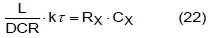
Figure 1 shows the configuration for DCR current sensing topology. The L is the inductor and the DCR is the DC resistance of the inductor. A current sensing resistor Rx and capacitor CX are in parallel with the inductor. Equation (3) shows the relationship between the inductor current and the VCX voltage. If you only consider the DC current signal, equation (3) can be rewritten as equation (4). Considering both the DC and AC signals, equation (3) can be rewritten as equation (5). By carefully designing the time constant of Rx and CX to satisfy the relationship L/DCR = RX*CX, the pole and zero in the DCR current sensing network will coincide and cancel each other. For this reason, both the DC and AC current signals obtained from VCX will be exactly same as IL*DCR.
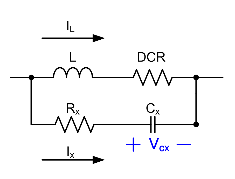
Figure 1. DCR Current Sensing Topology
Substitute (2) into (1)

Considering only the DC signal, (3) can be rewritten as (4).
From (3), considering both the DC and AC signals, (3) can be rewritten as (5):
Where  is defined as
2.
Introduction of Differential Current Sense Topology
Figure 2 shows the configuration for a differential current sensing topology. The inductor current is sensed as the voltage across the DCR current sense capacitor. Using the approximation that the op amp positive and negative input pins are a virtual short circuit, the VCX voltage is duplicated on the current sensing resistor, RCS, to transform the capacitor voltage VCX into an internal current signal. This per-phase current signal is used to do the per-phase current balance and per-phase over current protection. Then, the per-phase currents are mirrored by the current mirror circuits respectively and summed together to form the total current signal. The total current signal is injected into the RIMON resistor network. The RIMON network is connected between the IMON pin and the VREF pin and is used to decide the load-line droop, do the sum current reporting, and provide output over current protection and DCR temperature compensation.
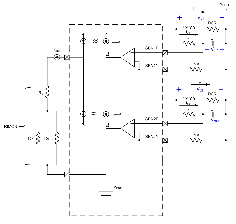
Figure 2. Differential Current Sense Topology
2.1 Derivation Procedure
of Differential Current Sensing Topology
Referring to Figure 2, the voltage across the inductor (VLn) can be expressed as the inductor current (ILn) product  . Therefore equation (6) can be rewritten as equation (7), and the capacitor current Ixn can be expressed as equation (8). Substituting equation (8) into equation (7), the relationship between the inductor current and the capacitor voltage can be expressed as equation (9).
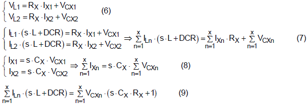
If the time constant of the Rx Cx sensing network is matched to the inductor’s Lx/DCR , equation (9) can be rewritten as equation (10). The Vcx voltage signals will be changed into current signals through the current sensing resistors Rcs, and the total sensed current can be expressed as equation (11). After that, the total sensed current is injected into the RIMON resistor network for temperature compensation. The ΔVIMON voltage is sensed for total current reporting and over current protection, and to determine voltage positioning load line droop or other purposes.
3.
Introduction of Sum Current Topology
Figure. 3 shows the sum current sensing topology. The sum current sensing topology uses an op amp as an adder to sum the DCR sensing capacitor voltages (VCXn).The current sensing resistors(RSn) change the sensing capacitor voltages (VCXn) into current signals (ISn) and the total current flows to the Rsum resistor network (which can perform any necessary temperature compensation). The total inductor current can be obtained by sensing the Vsum voltage. This current sense topology needs only three pins to sense the total inductor current, which greatly reduces the number of pins compared to the differential current sense topology.
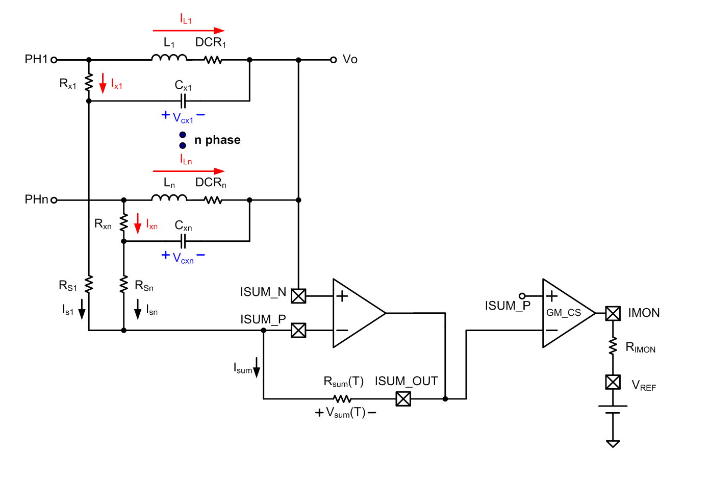
Figure 3. Sum Current Sensing Topology
To sense individual phase current signals, the sum current sensing topology needs an additional N pins for an N phase application. As Figure 4 indicates, the per-phase current signals use the common ISUM_N pin, reducing the IC pin count compared to differential sensing topologies.
In brief, the sum current sensing topology uses N+3 pins to sense both the sum current and per-phase current information. In multi-phase applications with more than 3 phases, the sum current sense topology can achieve pin savings compare to the differential current sense topology.
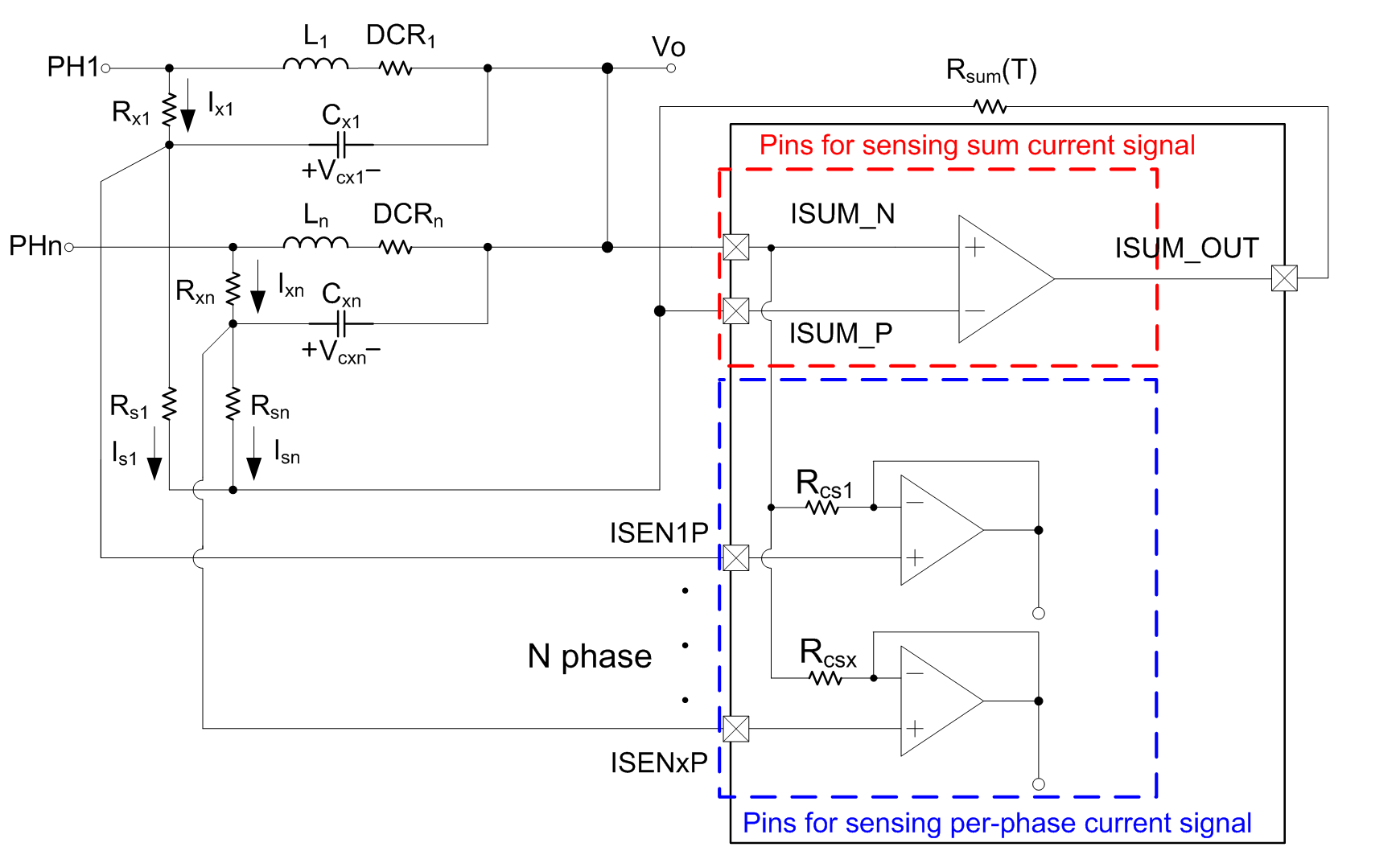
Figure 4. Per-phase Current Sense Circuit with Sum Current Topology
3.1
Derivation Procedure of Sum Current Sensing Topology
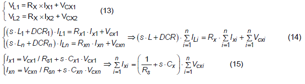
Refer to Figure. 3 and assume , for the final forms of equations (13), (14), (15) and (16). Substituting
  for VLn, the voltage across the inductor can be expressed as equation (14) and the capacitor current Ix can be expressed as equation (15). Substituting equation (15) into equation (14), the relationship between the inductor current and the capacitor voltage can be expressed as equation (16).
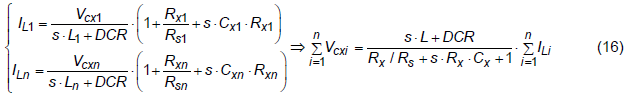
The Vsum equation can be obtained from Equation (17) and (18). After combining Equation (16) and (18), the relationship between Vsum and IL can be obtained in Equation (19).
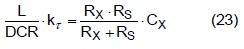
If the time constant of the (Rx//Rs)Cx sensing network is matched to the inductor’s Lx/DCR, equation (20) will apply and equation (19) becomes equation (21). Equation (21) shows that the Vsum value is proportional to the sum of the inductor currents.
4.
Comparison of the Differential and Sum Current Sensing Topologies
4.1
Pin Saving Capability
As mentioned above, the sum current sense topology uses an adder to sum the capacitor voltage of each DCR current sensing network. Therefore, it takes only 3 pins to get the total current information. Additionally, the sum current sense topology needs N pins to sense N per-phase current signals. Compare that to the differential current sense topology, which takes 2N pins to get N phase total current and per-phase current information. Obviously, as the phase number increases beyond 3, using the sum current sensing topology can achieve its pin saving purpose.
The differential current sensing topology can’t use the single ISENN pin due to the op amp virtual short characteristic. From Figure 2, if a single ISENN pin was used, it seems like two voltage sources (ISEN1P and ISEN2P) would be connected together. If these two voltages were different, this topology would violate the KVL rule. In a realistic application the voltage of these two points may not be the same since they sense inductor current from different phases.
4.2
Per-phase Current Accuracy
Though the total current can be precisely acquired through the sum current sensing topology and the differential current sensing topology, however, the per-phase current signal is not alike. The differential current sense topology can get precise per-phase current signals because it directly senses the DCR current sense capacitor voltage. Considering the PCB parasitic inductance and resistance between the ISEN_N input pins and the load VCORE point, a voltage spike will be induced at each ISEN_N pin when current passes through the parasitic elements. However, in the differential current sense topology this voltage spike will also be sensed at each ISEN_P pin and the differential value will not be affected. Figure 5 shows waveforms from a simulation, demonstrating that the sensed current remains accurate even though a voltage spike is induced at the ISEN_N pin.
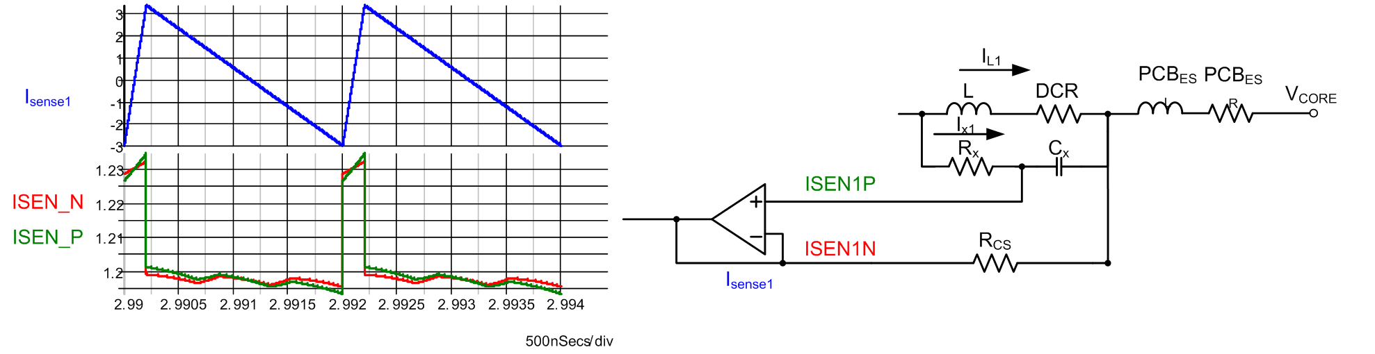
Figure 5. Parasitic Element Induced Voltage Spike at ISEN_N Pin and ISEN_P Pin
However, the sum current topology uses a common ISUM_N pin instead of per-phase ISEN_N pins to sense the per-phase current signals (Figure 3). Because the common ISUM_N pin is the average of each phase's sense capacitor negative terminal voltage, the ISUM_N voltage is slightly different from the differential topology ISEN_N point (capacitor) voltage. Especially considering the PCB parasitic inductance and resistance between the ISEN_N input pin and the load VCORE point. The Figure 6 simulation waveform (a) shows the sensed per-phase current waveform with the noise induced by the unwanted PCB parasitic parameters. Therefore, the per-phase current accuracy of the sum current sense topology may not be as good as the differential current sense topology.
However, some well-placed filter components can improve the performance of the sum topology. The filter components RF and CF can be added at each sense capacitor negative terminal, decoupling it from the output load point. This increases the layout complexity of the sum current sensing topology but significantly improves its per-phase accuracy. The Figure 6 simulation waveform (b) shows the sensed per-phase current waveform with the RF and CF filter components on each phase as shown in the circuit drawing.
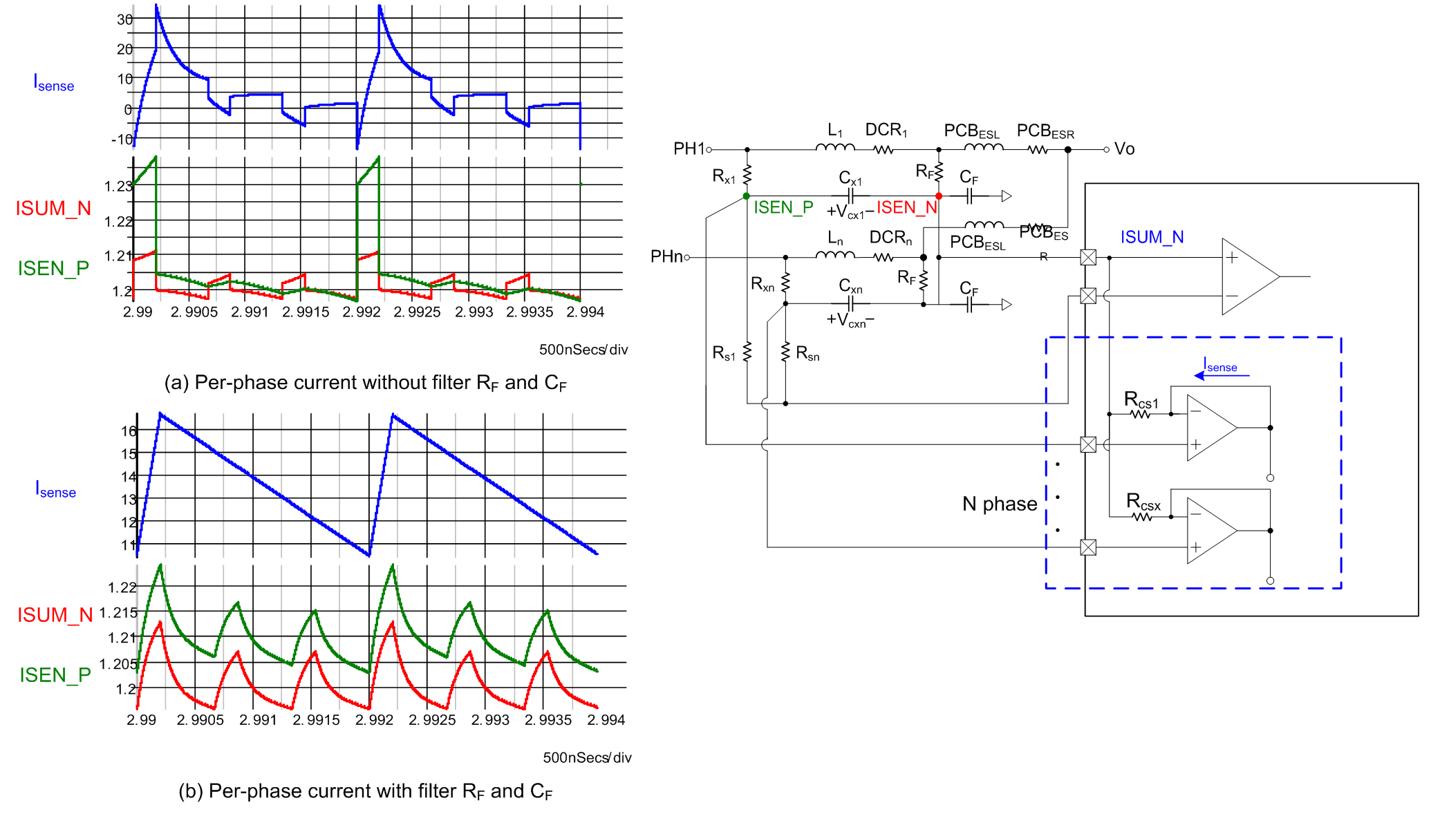
Figure 6. Sum Current Sense Topology with Parasitic Parameters
4.3 Tolerance
of Band (TOB) Analysis and Commercial Grade Temperature Specification
TOB Analysis:
The differential current sense method needs N current sensing op amps to convert the VCX voltage signals into current signals. Due to wafer process variations, the characteristics of each current sensing op amp may be different, such as input offset voltage, input bias current …etc. The offset voltage of the current sensing op amp may let the controller false detect the current level and regulate at the wrong voltage position, thereby lowering the output voltage and current reporting accuracy. To avoid this phenomenon, a self-calibration function is implemented in the IC during the IC start up procedure. Since the differential current sense method needs to calibrate N current sensing op amps, it is hard to increase the calibration resolution in the same IC die size. Therefore, the differential current sense method might have a larger offset voltage and need a tighter tolerance band to cover this issue.
However, in the sum current sense topology, there is only one current sense op amp in the total current signal path. Because only one op amp needs to be calibrated, the self-calibration resolution can be increased in the same IC die size, to reduce the op amp offset voltage. In the sum current topology the per-phase current signal, which is only used for current balance and per-phase over current protection, is not directly used to decide the output voltage positioning. Therefore, the TOB of the per-phase current sense op amp can be loosened and the slight mismatch between per-phase current sensing op amps is acceptable.
Commercial Grade Temperature Specification
Since the sum current sensing topology can use a higher self-calibration resolution to minimize the op amp input offset voltage, a wider operation temperature range can be adopted. Therefore, the sum current sensing topology can more easily pass the commercial grade temperature specification.
Table 1. Comparison of Differential and Sum Current Sensing Topologies
| |
Differential Current Sensing Topology
|
Sum Current Sensing Topology
|
|
IC Pin Count
|
Phase Number < 3
Better
|
Phase Number > 3
Better
|
|
Sum current accuracy
|
|
Better
|
|
Per-phase current accuracy
|
Better
|
|
|
PCBESR and PCBESL voltage spike noise immunity
|
Better
|
|
|
PCB layout complexity
|
Simple
|
Complex
|
|
Wafer process variation immunity
|
|
Better
|
|
Commercial Grade Temperature and TOB spec
|
|
Easier to pass
|
5.
Design Approach of Differential and Sum Current Topologies
The following design example will use the RT8884 for the differential current sense topology, and the RT8893 for the sum current sense topology. Both of these two ICs are designed to meet the Intel VR12.5 specification.
|
VCORE Specification
|
|
Input Voltage
|
10.8V to 13.2V
|
|
No. of Phases
|
3
|
|
Vboot
|
1.7V
|
|
VDAC(MAX)
|
1.8V
|
|
ICCMAX
|
90A
|
|
ICC-DY
|
60A
|
|
ICC-TDC
|
55A
|
|
Load Line
|
1.5mΩ
|
|
Fast Slew Rate
|
12.5mV/μs
|
|
Max Switching Frequency
|
300kHz
|
In Intel’s Shark Bay VRTB Guideline, the output filter requirements of the specification for a desktop platform are as follows:
Output Inductor: 360nH/0.72mΩ
Output Bulk Capacitor: 560μF/2.5V/5mΩ (max) 4 to 5pcs
Output Ceramic Capacitor: 22μF/0805 (18pcs max sites on top side)
Step 1 : Determine the Parameters of the Inductors
Output Inductor: 360nH/0.72mΩ
Step 2 : Determine the DCR Current Sensing Network Parameters
Choose the DCR current sensing capacitor (CX) value.
CX = 1μF
From experimental experience, using a 0.1µF capacitor the current sensing accuracy will degenerate at low current condition, so a 1µF capacitor is chosen.
Determine the DCR network time constant ratio, kt.
If the DCR network time constant ratio is less than 1, the capacitive time constant is less than the inductive time constant. This causes the AC current sense gain to be greater than the DC gain, increasing the DCR current sensing capacitor voltage (VCX) during the transient period. This causes voltage positioning overshoot and under shoot on load transients, and increases the possibility of incorrectly hitting the current limit. A ratio greater than 1 reduces sensed inductor ripple and transient current changes and will cause a sluggish voltage droop, but excessively small sensed inductor ripple can affect loop stability. Therefore, the DCR network time constant ratio is suggested to be equal to or slightly larger than 1. In this design example, the time constant ratio, kt, is chosen as 1. Figure 7 shows the simulation waveform during load transients. Three different DCR current sensing time constant ratio, 0.8, 1, 1.2, are used in the simulation to show the influence of Kt on the output voltage positioning and sensed current.
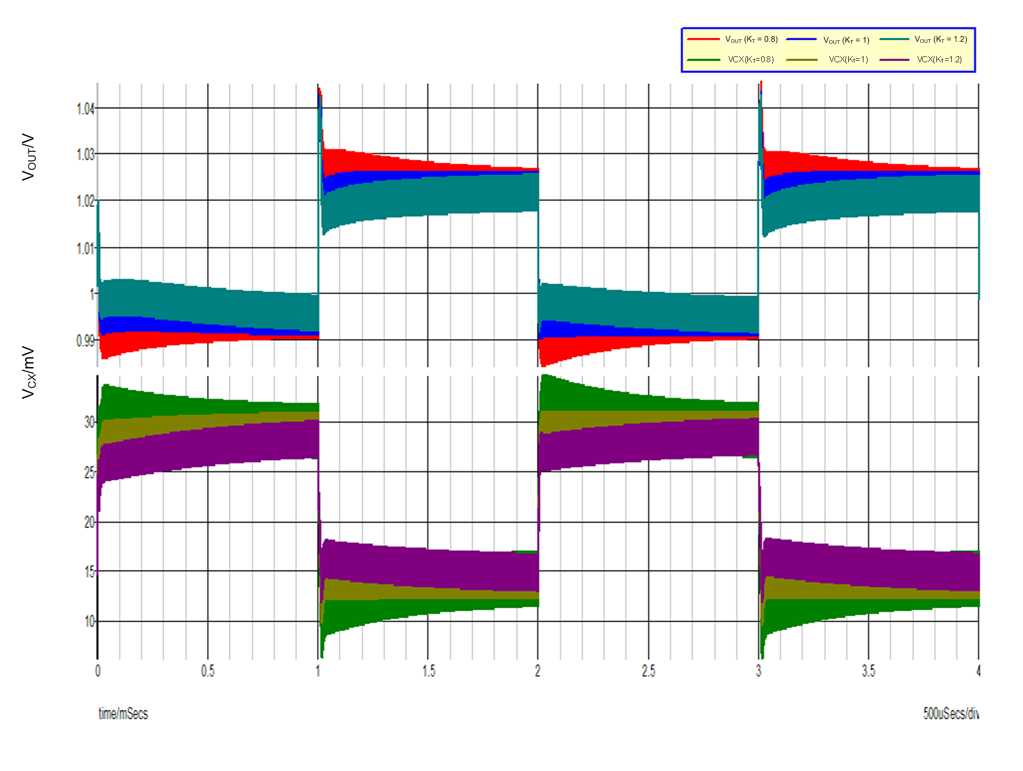
Figure 7 Output Voltage (VOUT) and VCX Voltage Load Transient Response with Various Kt Values
Differential current sense:
Sum current sense:
Step3: Calculate the RX and RS Values
Determine the RX and RS resistance values.
Differential current sense:
Sum current sense:
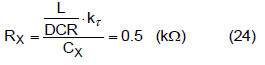
For sum current sensing op amp stability considerations, the ratio between Rsum and (RX + RS) is suggested to be4, and the Rsum value is suggested between 4kΩ~16kΩ.For the RT8893 application we choose Rsum = 16kΩ and the total resistance of (RX + RS) is therefore 4kΩ. Note, high resistance values reduce “the sum current sensing op amp phase margin. (For example: if (RX + RS) = 4kΩ and Rsum = 16kΩ, the sum op amp phase margin is about 45˚).
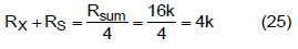
Using equation (23), the RX‧RS product value can be calculated.
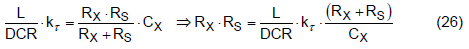
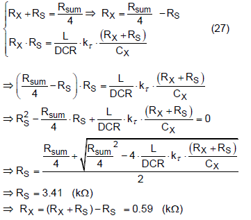
From (25) and (26), equation (27) can be used to find the RX and RS value. Substitute RX into RX‧RS, a RS second order equation can be derived. Substitute above mentioned parameter value into this equation and the RS can be found as 3.41kΩ and RX as 0.59kΩ.
6. Experimental Result
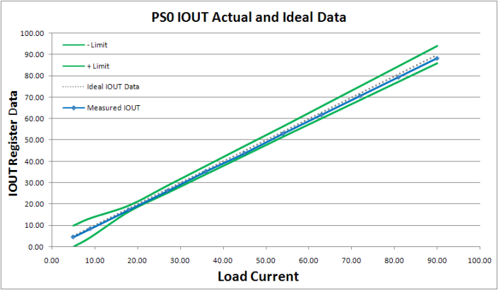
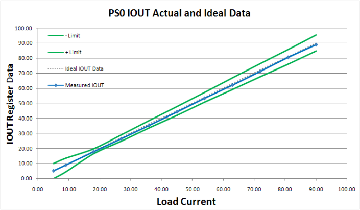
In a realistic application, the CPU will ask the VR to report the loading status. Therefore, the VR will change the sensed analog current signal into hexadecimal digital code, so-called as digital IMON (DIMON). If the DIMON is exactly the same as the loading current, we can judge that the VR can accurate sense the loading current. Figure 8 shows the DIMON current sense result using the two different current sense topologies. The dotted line is the ideal loading current signal, and the solid line is the reporting DIMON result. From the experimental results, both the sum current sense topology and differential current sense topology can deliver accurate total inductor current information.
|
(a)RT8884 differential current sense topology
|
(b)RT8893 sum current sense topology
|
Figure 8. DIMON current sense using two different current sense topologies
Figure 9 (a) shows the measured per-phase current sense signals with differential current sensing topologies, which shows that the differential current sensing topology features good per-phase current accuracy. Plot (b) shows the sum current sensing topology without the filter components. Since the sum current topology uses a common ISUM_N pin instead of directly sensing the negative terminal of the DCR capacitor, the per-phase current is not as accurate as the differential current sense topology. Plot (c) shows the sum current sensing topology with the filter components included. From the experimental result, the filter components can greatly improve the per-phase current accuracy, but is still inferior to differential sensing.
|
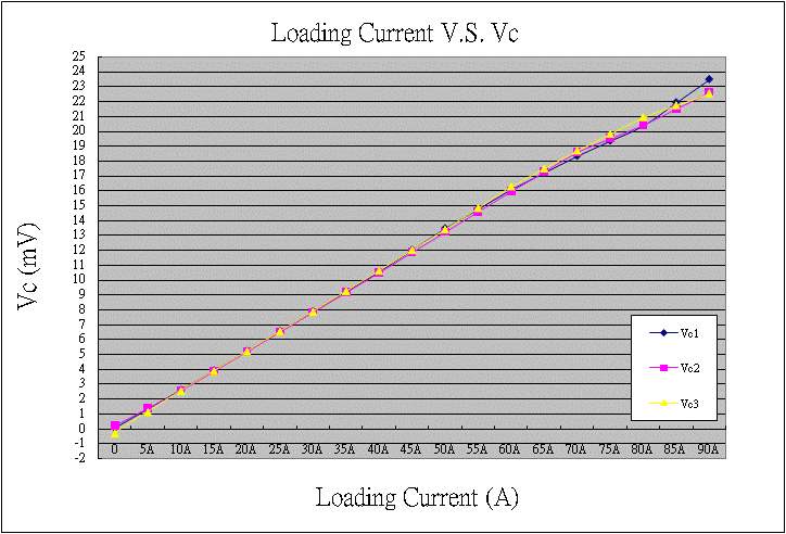
(a) RT8884 differential current sense topology
|
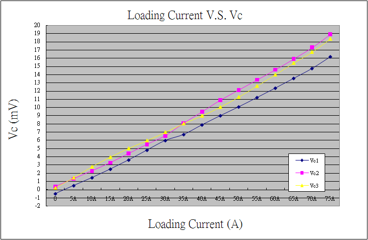
(b) RT8893 sum current sense topology w/o filter component
|
|
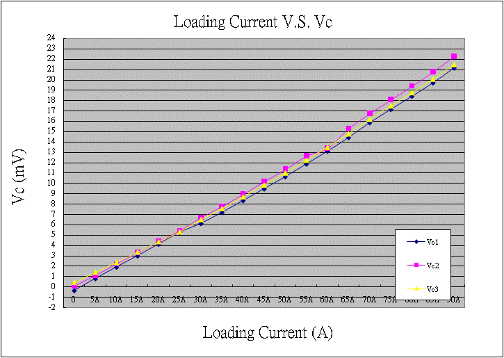
(c) RT8893 sum current sense topology with the filter component
|
Figure 9. Per-phase Current Signal with Various Current Sense Topologies
7.
Conclusion
This application note discussed two different kinds of current sense methods for multi-phase regulators. The sum current sense topology features better sum current accuracy, lower IC pin count, and more easily passes the TOB specifications. The differential current sense topology features better per-phase current accuracy and higher parasitic ESR and ESL noise immunity. In choosing a current sense topology, take into consideration your realistic application conditions, to find the most suitable current sense solution.
8.
Reference
[1] Richtek, RT8884B datasheet.
[2] Richtek, RT8893A datasheet.